Stress Photonics’ stress measurement systems work on a wide variety of silicon products, including silicon-coated glass, single crystal wafers, multicrystalline wafers, and micromachined devices. Most GFP™ (Grey-Field Polariscope) models can be made into silicon stress measurement tools with proper selection of NIR or SWIR cameras and compatible optics. A range of views, from large-area to microscopic fields-of-views, can be accomplished, either in real time or static to measure:
The GFP2600 NIR/SWIR Stress Measurement System, set at the edge of a test table or conveyor, can be configured as a very effective edge stress measurement tool. This versatile edge tool can move down the edge of the glass. Alternatively, the glass can be inspected as it moves through the edge stress measurement system.
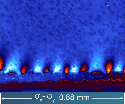
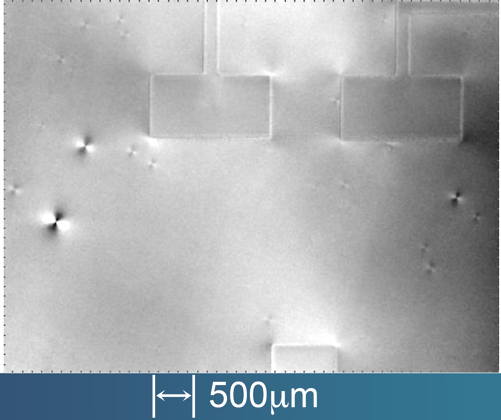
Laser Cut Edge of Si Wafer
The image above was acquired with the GFP™1500. The GFP™2600 Stress Measurement System is fully capable of acquiring the same stress image; however, with the GFP2600, image acquisition is instantaneous!
Stress near a crack at the edge of a single crystal Si wafer. Image acquired with the GFP™1500. The GFP™2600 system is fully capable of acquiring the same stress image; however, with the GFP2600, image acquisition is instantaneous!
Residual edge stress of a single crystal Si wafer. Image acquired with the GFP™1500. The GFP™2600 system is fully capable of acquiring the same stress image; however, with the GFP2600, image acquisition is instantaneous!
Stress from laser-drilled holes in Si Wafer. Image acquired with the GFP™1500. The GFP™2600 NIR/SWIR system is fully capable of acquiring the same stress image; however, with the GFP2600, image acquisition is instantaneous!
The GFP™2600real-time stress measurement system can be used to acquire area data in a scan configuration. A GFP2600 NIR/SWIRreal-time system, or a set of systems, acquires strip images as the wafer or coated glass moves by on a conveyor, or, for smaller products, a translation stage. The strip images are then “stitched” together using special software to form complete stress maps. The illumination is set up in transmission.
Other camera models, such as the GFP1500, have also been converted to silicon inspection systems upon request. Contact Stress Photonics for details.
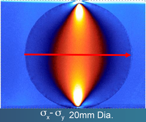
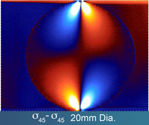
Si Disk in Diametral Compression
The image above was acquired with the GFP™1500. The GFP™2600 Stress Measurement System is fully capable of acquiring the same stress image; however, with the GFP2600, image acquisition is instantaneous!
The image above was acquired with the GFP™1500. The GFP™2600 Stress Measurement System is fully capable of acquiring the same stress image; however, with the GFP2600, image acquisition is instantaneous!
Stress in Si in four-point bend sample. The image above was acquired with the GFP™1500. The GFP™2600 system is fully capable of acquiring the same stress image; however, with the GFP2600, image acquisition is instantaneous!
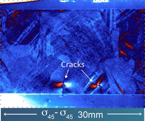
Crack detection via stress in multicrystalline Si wafer. Image acquired with the GFP™1500. The GFP™2600 system is fully capable of acquiring the same stress image; however, with the GFP2600, image acquisition is instantaneous!
Stress from laser-drilled holes in Si Wafer. Image acquired with the GFP™1500. The GFP™2600 NIR/SWIR system is fully capable of acquiring the same stress image; however, with the GFP2600, image acquisition is instantaneous!
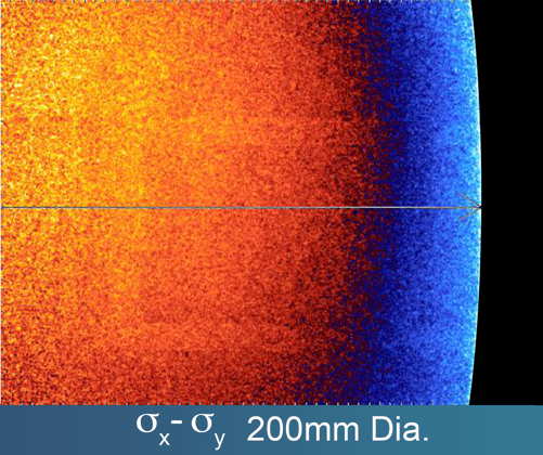
GFP™2600 NIR/SWIRreal-time stress measurement systems can assess thermal stresses due to processes on wafers or coated plates. Typically, the product must be transparent to some wavelength of light up to 1700 nm (SWIR).
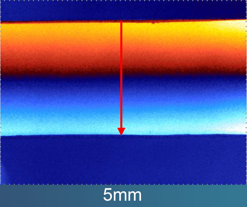
Multicrystalline Si Wafer Thermal Stress
The image above was acquired with the GFP™1500. The GFP™2600 Stress Measurement System is fully capable of acquiring the same stress image; however, with the GFP2600, image acquisition is instantaneous.
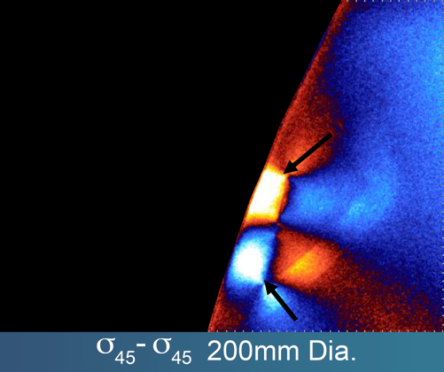
GFP™2600 NIR/SWIRreal-time stress measurement systems can assess defects in silicon wafers, such as dislocations and laser cuts, or defects in the coating or coated plates. The systems can also measure the polarization associated with crystal orientation. Typically, the article must be transparent to some wavelength of light up to 1700nm (SWIR).
Laser Cut Edge of Si Wafer
The image above was acquired with the GFP™1500. The GFP™2600 Stress Measurement System is fully capable of acquiring the same stress image; however, with the GFP2600, image acquisition is instantaneous!
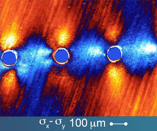
Contact stress of trapped particles of anodic-bonded Si structure. Image acquired with the GFP™1600 FPI. The GFP™2600 is also capable of acquiring the same stress image; however, with the GFP2600, image acquisition is instantaneous!
Crack detection via stress in multicrystalline Si wafer. Image acquired with the GFP™1500. The GFP™2600 system is fully capable of acquiring the same stress image; however, with the GFP2600, image acquisition is instantaneous!
Stress near a crack at the edge of a single crystal Si wafer. Image acquired with the GFP™1500. The GFP™2600 system is fully capable of acquiring the same stress image; however, with the GFP2600, image acquisition is instantaneous!
Polarization due to crystal orientation of Si wafer. Image acquired with the GFP™1500. The GFP™2600 system is fully capable of acquiring the same stress image; however, with the GFP2600, image acquisition is instantaneous!
Residual edge stress of a single crystal Si wafer. Image acquired with the GFP™1500. The GFP™2600 system is fully capable of acquiring the same stress image; however, with the GFP2600, image acquisition is instantaneous!
Stress from laser-drilled holes in Si Wafer. Image acquired with the GFP™1500. The GFP™2600 NIR/SWIR system is fully capable of acquiring the same stress image; however, with the GFP2600, image acquisition is instantaneous!