The GFP™2600 NIR/SWIR Real-time Photoelastic Stress Analysis (PSA) System instantaneously measures stress through NIR/SWIR transparent materials such as silicon wafers, silicon coated glass, and many ceramics. Systems include a NIR/SWIR circularly polarized illuminator and an analyzing camera. Cameras can be configured to provide an area field of view (FOV) or a strip FOV. The strip data can be stitched together to create extremely large images.
The cameras are fixed focal length, but can focus close to find small defects such as particles trapped between bonded wafers, or they can focus far to inspect whole wafers. Similarly, for silicon coated glass, you can focus close on edge stress or far to inspect the full width. The specific camera, NIR (750–1000nm) or SWIR (1000–1700nm), is selected in combination with a bandpass filter to optimize performance for a given material or application.
Full-Featured Software
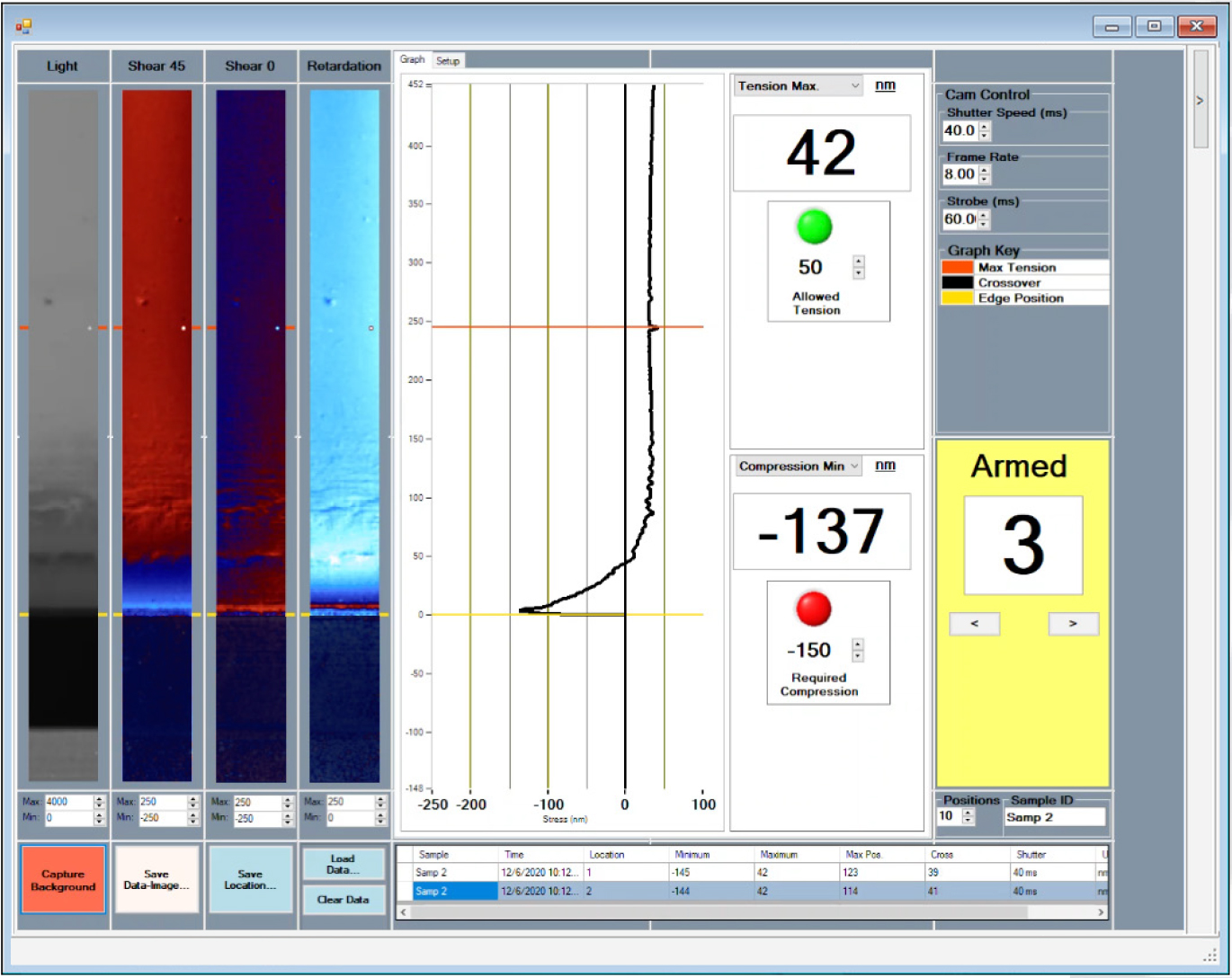
The GFP2600 NIR/SWIR Photoelastic Stress Analysis (PSA) System is managed with easy-to-use software. The software is a versatile tool for capturing, presenting, analyzing, and archiving photoelastic data. Retardation images can be saved for further
processing via Stress Photonics’ DeltaVision™ data viewing software, or line plots can be logged and
later viewed in spreadsheets.
Software Features
Among many other features, the software provides:
Live Image Monitoring
Image Acquisition and Controls
Data Interrogation such as Live Line Plot
Limit Checking of Max and Min Retardation Values
Reference Image Subtraction
Data Smoothing
Conversion to Stress Images
Edge Stress of Coated Glass
GFP2600 NIR/SWIR Applications
The GFP2600, in conjunction with the NIR/SWIR Illuminator, allows for full-field stress images of transparent materials such as silicon wafers, silicon coated glass, and many ceramics. Easily collect accurate and quantifiable stress data over whole wafers or focus close to find small defects such as particles trapped between bonded wafers to solve problems in manufacturing or to create a database of stress information.
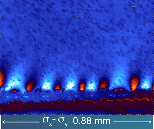
Laser Cut Edge of Si Wafer
The image above was acquired with the GFP™1500. The GFP™2600 Stress Measurement System is fully capable of acquiring the same stress image; however, with the GFP2600, image acquisition is instantaneous!
Contact stress of trapped particles of anodic-bonded Si structure. Image acquired with the GFP™1600 FPI. The GFP™2600 is also capable of acquiring the same stress image; however, with the GFP2600, image acquisition is instantaneous!
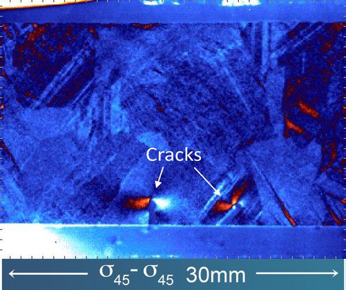
Crack detection via stress in multicrystalline Si wafer. Image acquired with the GFP™1500. The GFP™2600 system is fully capable of acquiring the same stress image; however, with the GFP2600, image acquisition is instantaneous!
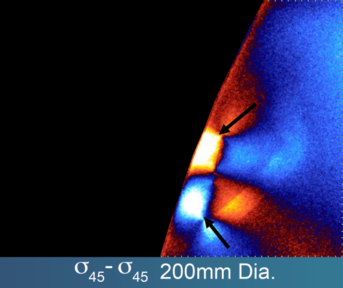
Stress near a crack at the edge of a single crystal Si wafer. Image acquired with the GFP™1500. The GFP™2600 system is fully capable of acquiring the same stress image; however, with the GFP2600, image acquisition is instantaneous!
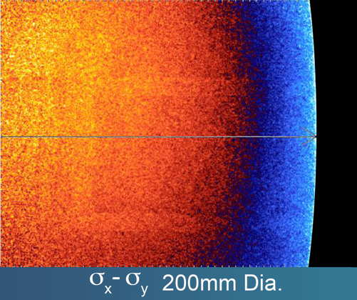
Residual edge stress of a single crystal Si wafer. Image acquired with the GFP™1500. The GFP™2600 system is fully capable of acquiring the same stress image; however, with the GFP2600, image acquisition is instantaneous!
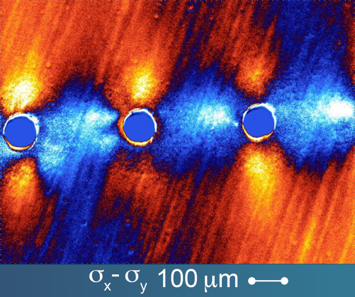
Stress from laser-drilled holes in Si Wafer. Image acquired with the GFP™1500. The GFP™2600 NIR/SWIR system is fully capable of acquiring the same stress image; however, with the GFP2600, image acquisition is instantaneous!
Specifications are general. Definitive specifications are determined by application and will be reflected in final quote.
Powerful Algorithms
The GFP2600 NIR/SWIR Real-time Photoelastic Stress Analysis System acquires instantaneous stress images or videos via kaleidoscopic optics. The system creates multiple copies of the stress images—all exposed to different sets of polarizing optics. Powerful algorithms process the images to produce real-time photoelastic stress images. The results are based on two fundamental images referred to as:
Shear 0—The in-plane shear strain on the 0° (horizontal) axis
Shear 45—The in-plane shear strain on the 45° orientation
Shear 0—The in-plane shear strain on the 0° (horizontal) axis
Shear 45—The in-plane shear strain on the 45° orientation
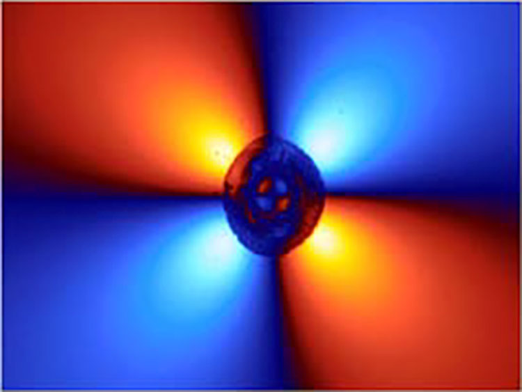
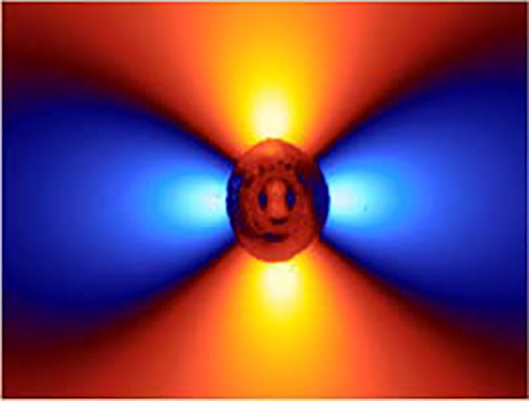
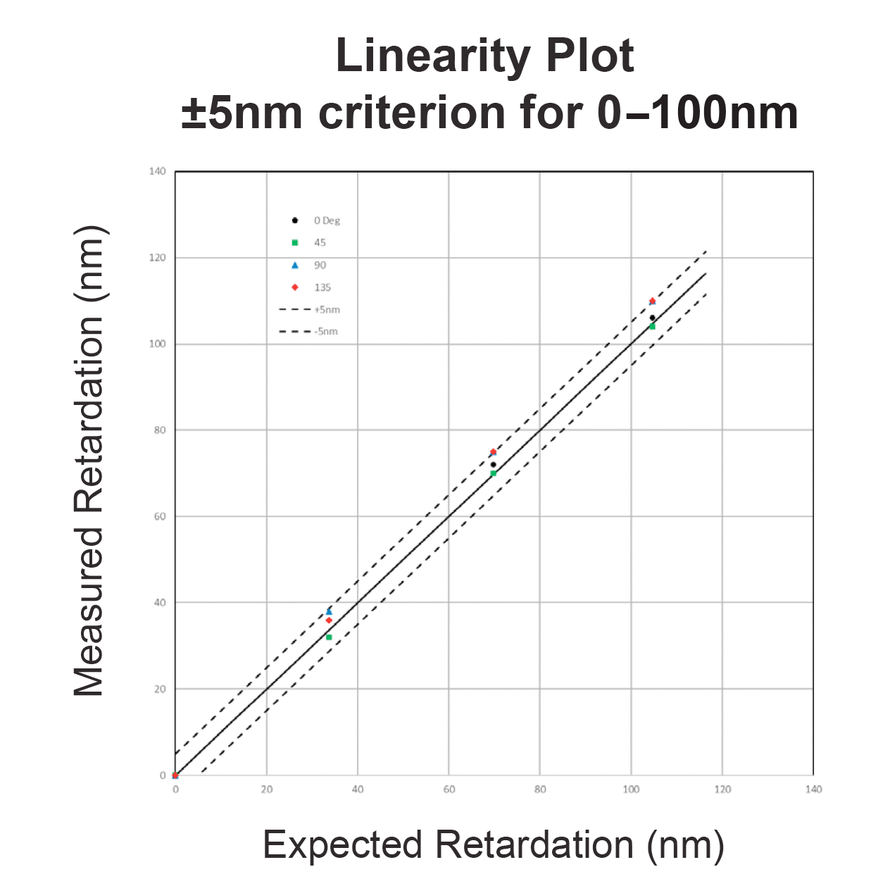
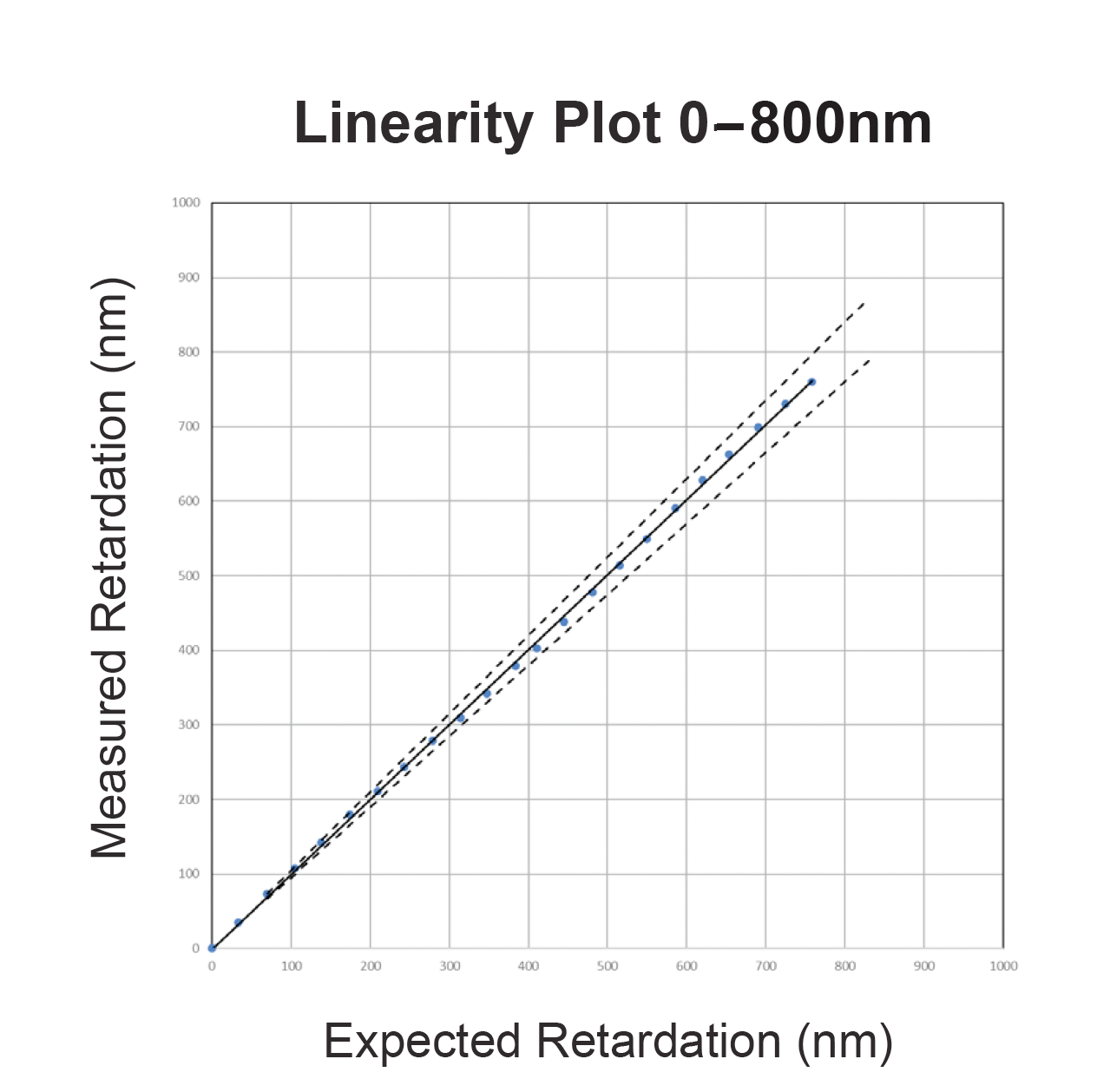
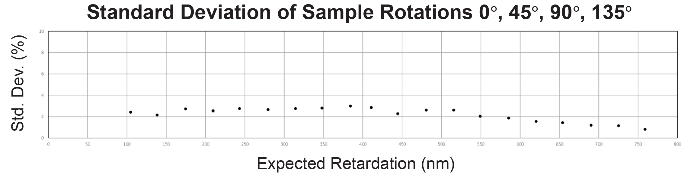
Calibration Tests
Tests performed with calibration plates viewed through silicon coated glass.
All Sample Rotations (Plot lower left.)
Average of 4 Cal Sample Rotations 0°, 45°, 90°, 135° (Plot lower right.)
Shear 0—The in-plane shear strain on the 0° (horizontal) axis
Shear 45—The in-plane shear strain on the 45° orientation
Shear 0—The in-plane shear strain on the 0° (horizontal) axis
Shear 45—The in-plane shear strain on the 45° orientation
Repeatability Test
Tests performed with calibration plates viewed through silicon coated glass.